
New Metasurface Technology Boosts Light Frequency Conversion
Scientists in Austria and the United States have developed a new method for converting light into different frequencies. This breakthrough involves combining special layered materials with a nanostructure called a metasurface to improve how light interacts with matter. The new device can change the frequency of light, including wavelengths that are important for telecommunications and quantum communication systems. The research was published September 2 in Nature Nanotechnology.
Nonlinear frequency conversion is a process where light enters a material and changes into a different color or energy level. This method is already used in many modern technologies like lasers, signal processors, and systems that create entangled photons for secure communication. The specific type of conversion used in this new study is called second-harmonic generation. In this process, two photons interact to produce light with twice the frequency and twice the photon energy. Materials used for this process often have relatively weak nonlinear responses. This can make it difficult to build small and efficient devices.
A research team at the University of Texas at Austin created a material using layers of gallium arsenide and aluminium gallium arsenide, according to Physics World. These layers form what are known as quantum wells that confine charge carriers in one direction while allowing them to move more freely in the other two. The researchers coupled quantum wells of different widths to create an asymmetric structure. This asymmetry produces a large electron displacement during certain optical transitions and strengthens the material’s nonlinear response.
Marcus Ossiander from TU Graz and his colleagues added another component to the setup by placing a metasurface on top of the quantum-well structure. This layer is made of titanium dioxide pillars that are hundreds of nanometers tall and help control how light enters the structure. The pillars were about 390 nanometers tall in the device described by the researchers. The design creates a guided-mode resonance that concentrates and controls the electric field inside the material.
Researchers had previously known that metasurfaces can trap light and make it interact more closely with matter. However, the team designed the new structure to do more than simply strengthen the incoming light. It also creates the combination of electric-field directions needed to access the unusually strong nonlinear response of the quantum wells.
The researchers measured an effective second-order nonlinear susceptibility of about 14 nanometers per volt. That was more than 270 times the largest comparable nonlinear tensor element of lithium niobate used as a reference in the study. The metasurface increased the relevant electric-field product inside the quantum-well structure by about 57 times compared with the unpatterned material under the researchers’ comparison conditions.
The device operated with a pump wavelength near 1.57 micrometers. That wavelength is in the near-infrared range and is close to wavelengths widely used in optical telecommunications. The experiment produced second-harmonic light at about half that wavelength.
Marcus Ossiander explained that nonlinear optics are important for many modern technologies. These include creating new light sources, processing signals with light, and making entangled photons for secure communication. The researchers said their approach could also be adapted for processes including difference-frequency generation and spontaneous parametric downconversion.
Pernille Undrum Fathi from Harvard’s engineering school was one of the lead researchers on this project. Researchers from Harvard University, the University of Texas at Austin, the University of California Irvine, Sandia National Laboratories, MIT, Caltech, ETH Zurich and TU Graz contributed to the work.
The team’s work shows how combining different materials can lead to new and better ways of using light in technology. This research could help make smaller and more efficient components for future communication and computing systems. The researchers said the design provides a scalable route toward compact nonlinear-photonic devices.
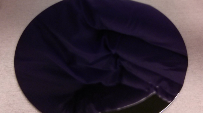
IMAGE: Gallium Arsenide (GaAs) 2″ wafer La2O3 CC3